Applications of HDI PCB Technology
The advancements in electronic devices have resulted in shrinking form factors and higher functionality. Consequently, the dimensional spacing for circuit board traces or pads has also reduced (known as the pitch). The shrinking of package size of Integrated Circuits (ICs) necessitates the use of high-density PCBs with smaller pitches to facilitate interconnection of the ICs. The use of HDI technology also reduces manufacturing costs and increases the reliability of the resulting product.
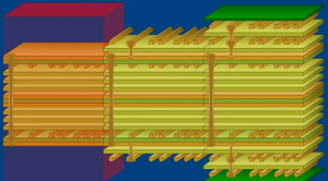
HDI PCBs feature lower layer counts, thinner traces and microvias that are smaller than traditional through holes. These advanced features enable more components to be integrated into a single circuit board, and help improve signal quality. However, the increased circuitry density comes with challenges, such as the need to carefully consider material selections for signal integrity and impedance control. In addition, careful consideration of component placement and layout is required to achieve superior performance and stability in HDI boards.
The use of HDI PCBs is growing in popularity for a wide range of electronic applications. One of the most prominent uses is for medical devices, where the smaller size can improve performance and allow for more features to be included in a device. Pacemakers are a great example of this. hdi pcb are also used in a variety of other medical devices, including imaging equipment, surgical instruments and monitoring systems.
What Are the Typical Applications of HDI PCB Technology?
Another significant application of HDI PCBs is in the automobile industry. As cars become more and more connected, they require more complex and reliable computerized components. HDI PCBs are a critical component in many of these systems, and the smaller size can help reduce weight and enhance vehicle performance.
Moreover, HDI PCBs are well-suited for military and aerospace applications where the devices need to operate in harsh and hazardous environments. The high-density circuitry allows for more functions to be combined into a smaller, lighter and more compact device.
Faster production times: The design efficiencies linked with HDI PCB technology allow for shorter timeframes to get your product to market. The ease of placing components, the reliability of microvias and improved electrical performance reduce the testing and troubleshooting time needed to optimize your design for manufacturing.
Cost-effective in the long run: The reduced layer count and smaller size of HDI PCBs can lead to more efficient circuitry, reducing overall production costs. Additionally, the reduced thickness of HDI boards can result in a more lightweight and compact final product, further lowering the total manufacturing cost.
Optimizing the Layer Count: When designing a multilayer HDI PCB, it is important to keep in mind that higher layer counts increase manufacturing complexity and cost. Therefore, it is recommended to choose the smallest possible layer count for your specific needs.
Choosing the right material is also essential for high-performance HDI PCBs. In order to maintain good signal quality, you should select materials that offer optimal dielectric properties. This includes considering their coefficient of thermal expansion (CTE), conductivity, and performance under stress.